
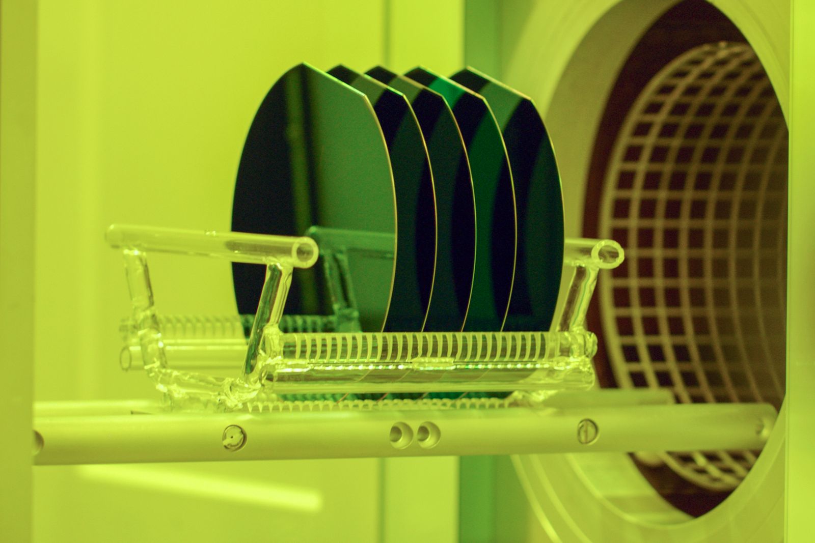
Foundry services
From shared prototyping wafers to industrial-scale production, all on one industrial TFLN platform built in Neuchâtel.
What we fabricate
Monolithic TFLN chips
Fabricated on lithium niobate on insulator (LNOI) substrates with up to ten main process steps for full photonic integration.
TFLN chiplets
Compatible with micro-transfer printing for cost-effective, scalable heterogeneous integration.
TFLN-enhanced silicon photonics
TFLN micromachining for silicon photonics fabs and platform developers adding TFLN to their flow.
Ongoing R&D with CSEM
CSEM keeps advancing the platform through process innovation, device integration and collaborative research.
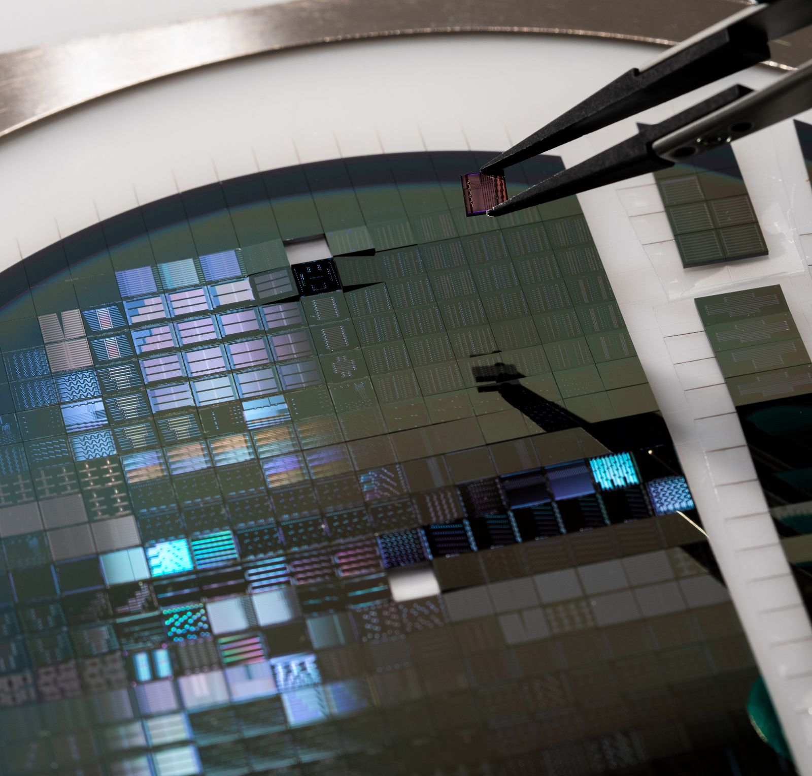
Multi-project wafer runs
Access high-performance TFLN at low cost by sharing wafer area. Built on our standardized platform and process design kit, ideal for proof-of-concept designs and academic projects.
- Ideal for
- Prototyping, research, early-stage validation
- Volume
- Shared wafer access
- Cost
- Entry level, per mm²
| Run | Technology | Design due | Status |
|---|---|---|---|
| 2601 | CLN-Core | 28 Feb 2026 | Closed |
| 2602 | CLN-Plus | 30 Apr 2026 | Closed |
| 2603 | CLN-Core | 31 Aug 2026 | Closed |
| 2604 | CLN-Plus | 15 Dec 2026 | Accepting designs |
| 2701 | CLN-Core | 21 Mar 2027 | Accepting designs |
| 2702 | CLN-Plus | 21 Mar 2027 | Accepting designs |
| 2703 | CLN-Core | 21 Sep 2027 | Accepting designs |
| 2704 | CLN-Plus | 21 Sep 2027 | Accepting designs |
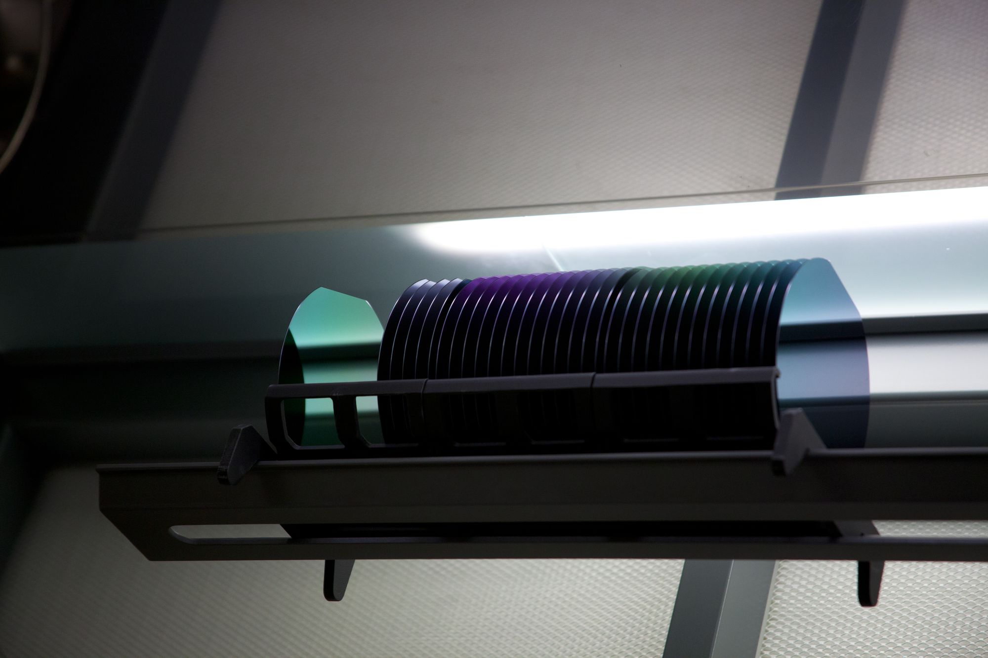
Custom dedicated wafer runs
When your design needs more space, tailored process steps or serves a niche market, dedicated runs give you full control over layout, integration and fabrication parameters. Ideal for qualification before high-volume production.
- Ideal for
- Pre-production, product integration, process qualification
- Volume
- Dedicated wafers, minimum 4
- Cost
- Per wafer or per chip, by order size
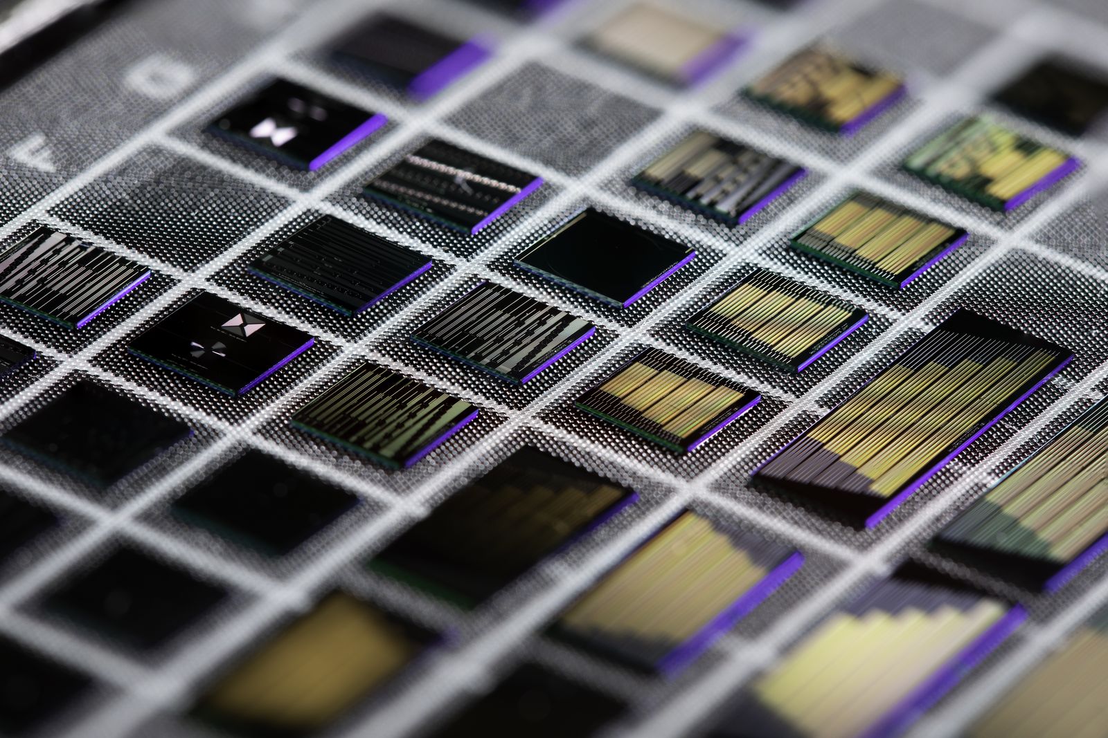
High-volume TFLN manufacturing
We already manufacture and deliver TFLN chips through MPW and dedicated runs. We are now establishing a dedicated TFLN fab, with reproducible processes and consistent quality, to scale production to 2,000 wafers per month.
- Ideal for
- Industrial-scale photonic chip production
- Target capacity
- 2,000 wafers per month
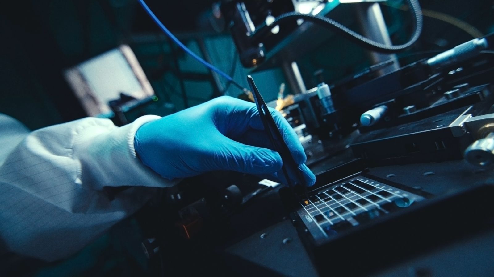
Specialty process services
Targeted fabrication steps on TFLN and related materials: etching, metal deposition, oxide deposition and periodic poling, from prototype engagements to volume production.
- Ideal for
- Platform developers, foundries, R&D partners
- Volume
- From 4 wafers
- Cost
- Project based
Process and PDK
Our proprietary process serves fabless early adopters of TFLN and silicon photonics foundries adding TFLN to their platforms.
- Precision TFLN micromachining
- Multilayer metallization
- Cladding and layer openings
- Device-layer undercut
- Electro-optic modulators
- Low-loss fiber coupling
- Frequency conversion via PPLN
- Acousto-optic modulation
C-band, 1550 nm
Qualified
Tested through several runs, with ongoing maintenance and new building blocks.
O-band, 1310 nm
Alpha, under test
Beta version launching in 2026.
Quantum and visible, 500 to 900 nm
Alpha, under test
Beta version launching in 2026.
PDKs for the CCRAFT platform are also available in Luceda Photonics' design environment.