
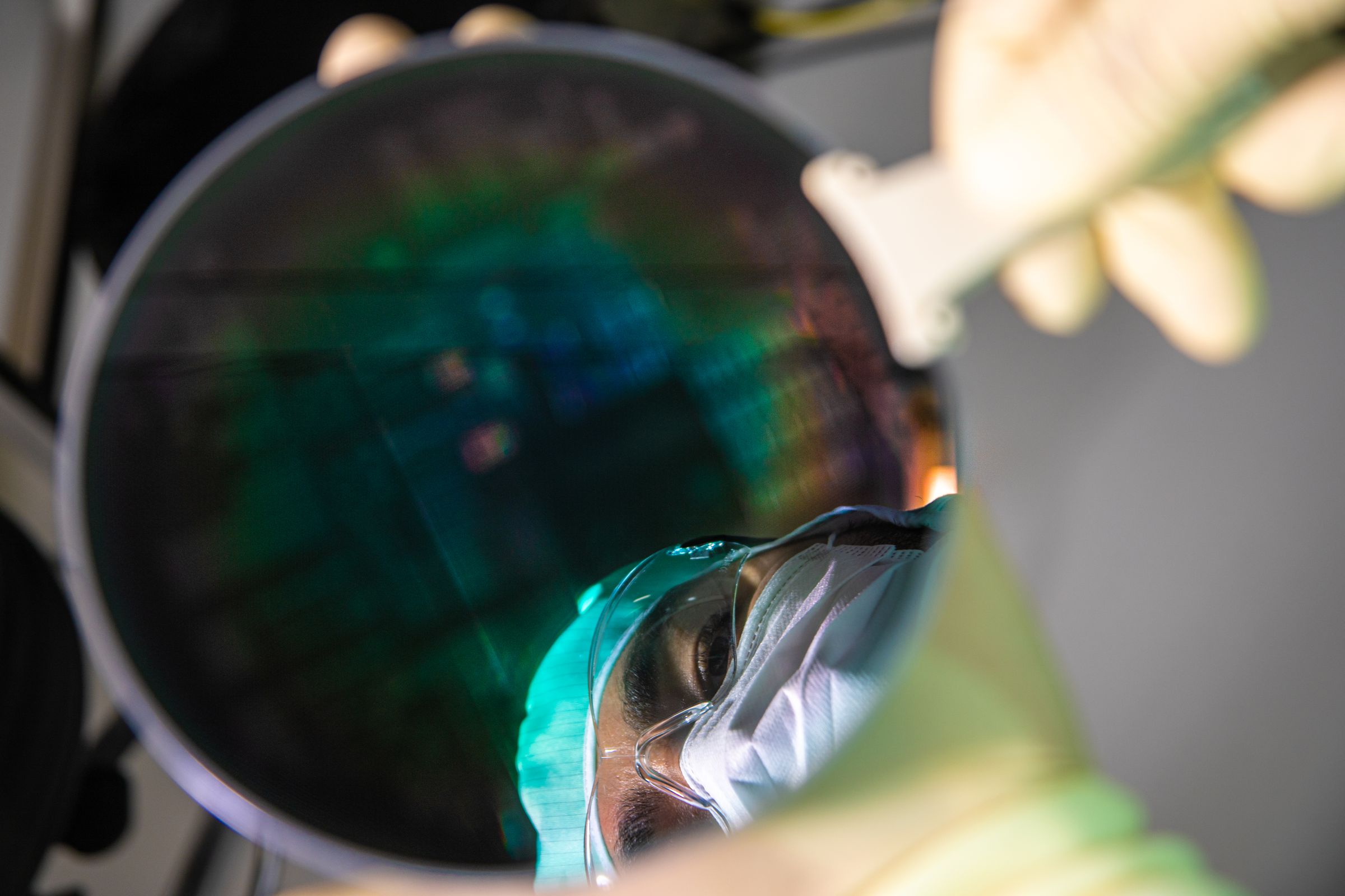
Thin-film lithium niobate chips, fabricated in Neuchâtel
CCRAFT is the independent pure-play TFLN foundry. MPW, custom and volume runs on 150 mm wafers for photonic chip designers in telecom, AI, quantum and space.
See the next MPW runLight enters the chip
An optical signal couples into a waveguide etched in thin-film lithium niobate. A junction splits it into two arms.
The crystal follows the voltage
Gold electrodes run along both arms. Lithium niobate changes its refractive index with the applied field, so the phase in each arm follows the drive signal.
Data leaves at over 400 Gbit/s
Where the arms meet again, the phase difference decides which output the light takes. That is how our modulators switch, at CMOS-level drive voltages.
Why design teams fab with CCRAFT
Six years of TFLN R&D at CSEM and thousands of pilot-line chips for more than 40 partners, now an industrial foundry serving customers on four continents.
Read our storyLithium niobate has been a telecom material for decades. In thin film it brings fast, low-power electro-optic modulation onto a chip, and we run it as a qualified, repeatable foundry process.
Beyond 400 Gbit/s
TFLN electro-optic modulators for high-speed links across the O, S, C and L bands.
CMOS-level drive voltages
Low-power modulation with simplified electronics, ready for co-packaged optics and 3D stacking.
ISO 9001 and 14001, 150 mm
A certified wafer foundry in the heart of Europe, with confidentiality built into every run.
A PDK tested over many runs
Qualified C-band building blocks, with O-band and visible to NIR kits in alpha testing.
Foundry services
From a shared wafer for your first prototype to dedicated lines for volume production. Every route runs on the same industrial TFLN platform.
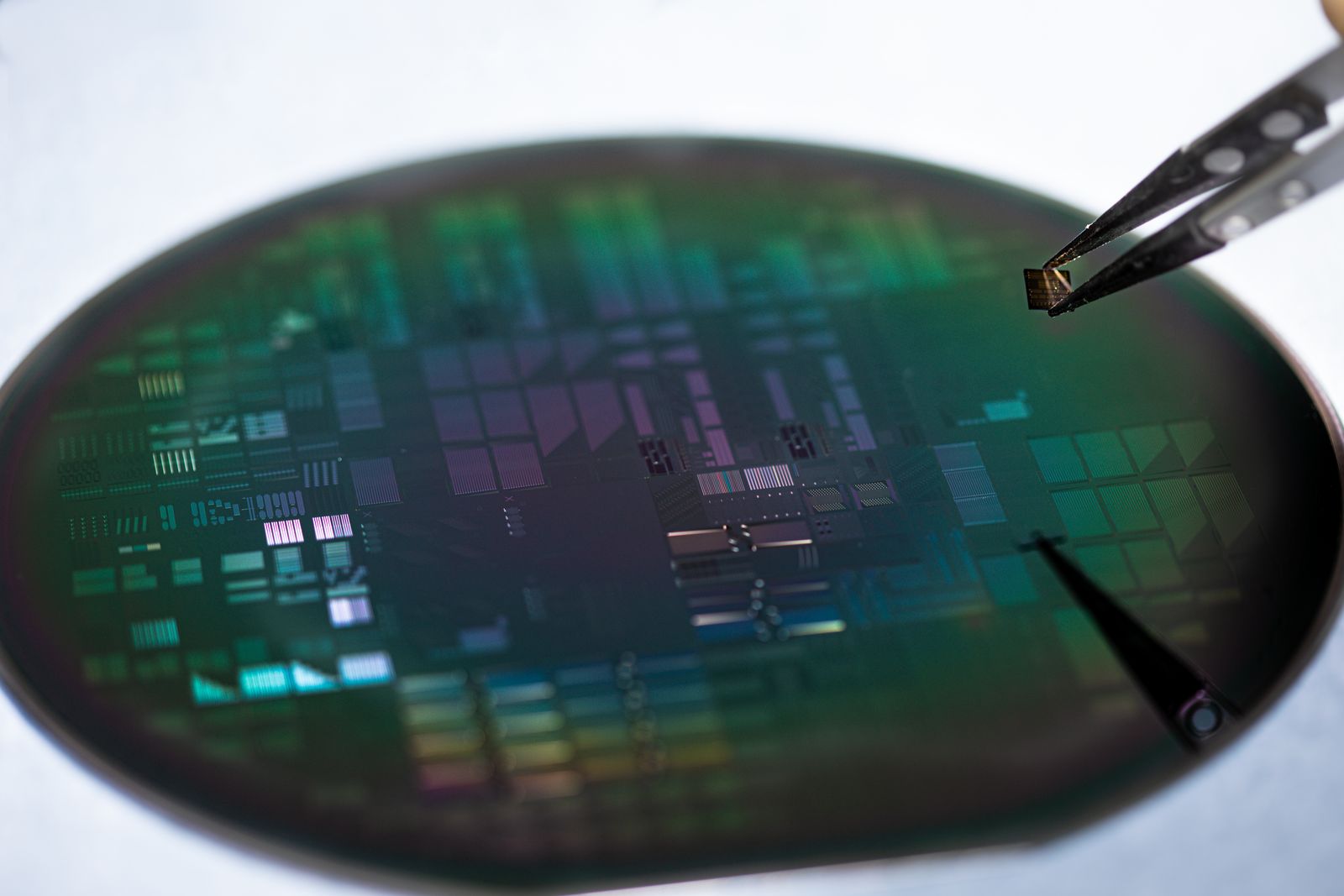
Multi-project wafer
Share wafer area on our standardized platform and PDK.
- For
- Prototyping, research
- Cost
- Entry level, per mm²
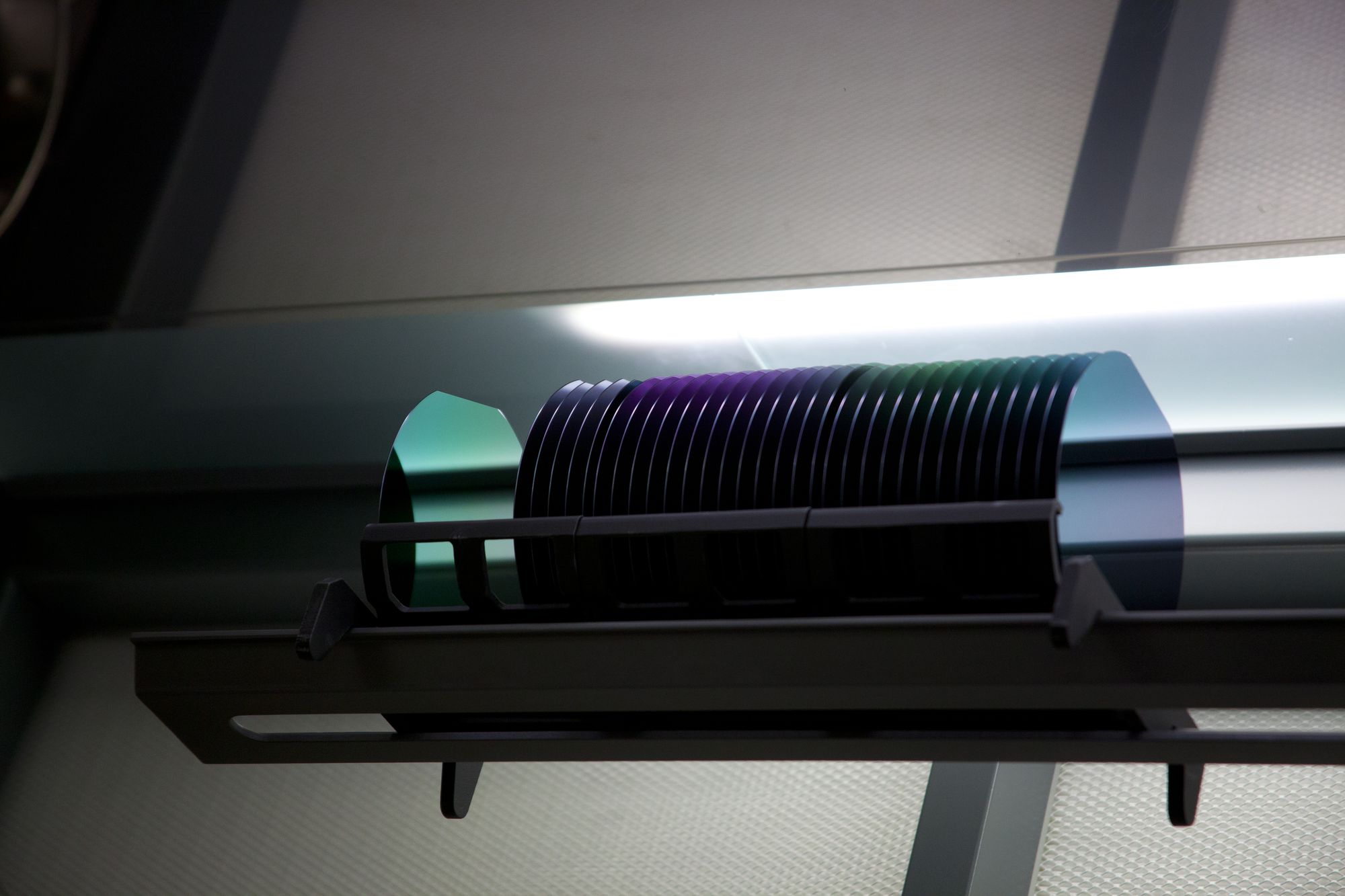
Custom wafer runs
Dedicated wafers with full control over layout and process.
- For
- Pre-production, qualification
- Volume
- From 4 wafers
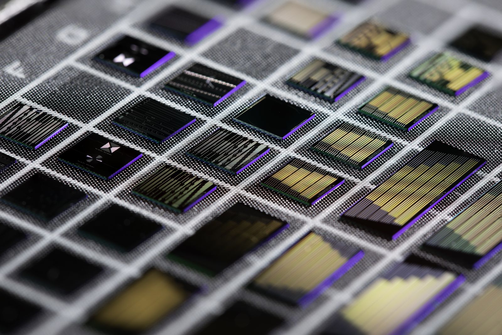
High-volume manufacturing
A dedicated TFLN fab scaling to 2,000 wafers a month by 2030.
- For
- Industrial-scale production
- Target
- 2,000 wafers/month
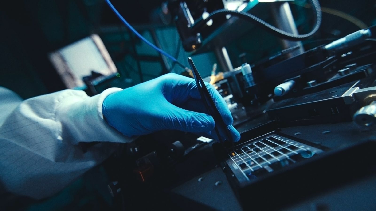
Specialty process services
Etching, metal and oxide deposition, periodic poling.
- For
- Fabs, platform developers
- Volume
- From 4 wafers
Next MPW runs
Three to four runs a year on our CLN-Core and CLN-Plus technologies. Participation is limited, so early registration is recommended.
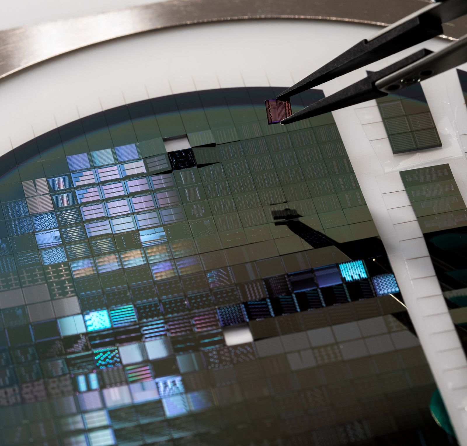
Design due for run 2604 on CLN-Plus, 15 Dec 2026
| Run | Technology | Design due | Status |
|---|---|---|---|
| CLN-Plus | 15 Dec 2026 | Accepting designs | |
| CLN-Core | 21 Mar 2027 | Accepting designs | |
| CLN-Plus | 21 Mar 2027 | Accepting designs | |
| CLN-Core | 21 Sep 2027 | Accepting designs |
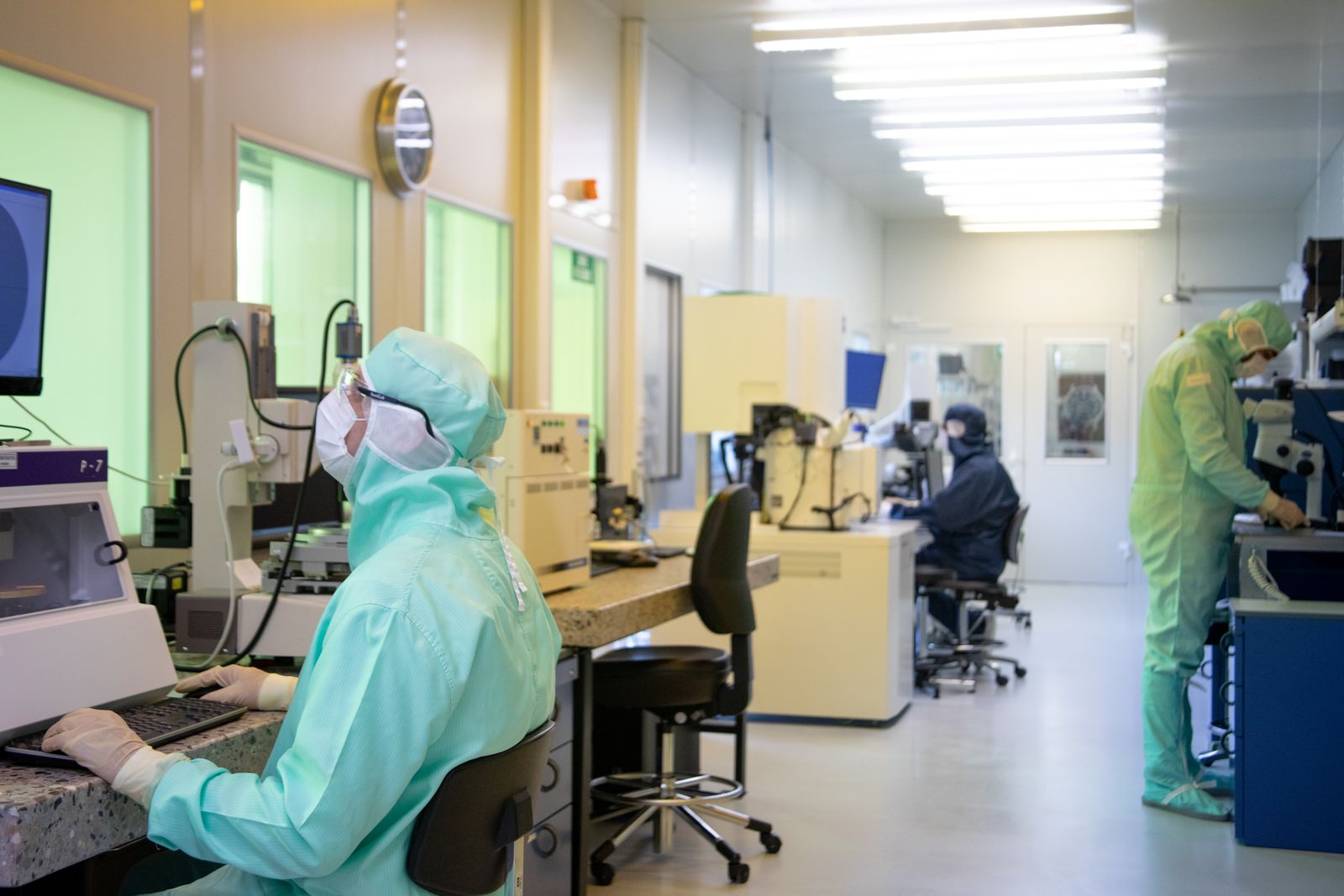
Cleanroom and characterization lab, Neuchâtel
Milestones
Before 2025
- More than six years of TFLN process development at CSEM, Neuchâtel
- Thousands of chips delivered to over 40 partners through the pilot line
2025
- CCRAFT launches as the first production-ready TFLN foundry
- Best ICT Startup at the Swiss Venture Competition
- Two new PDKs released with Luceda Photonics
- Innosuisse support for photonic chips for AI data centers
2026
- Audience Award at the ZKB Pionierpreis Technopark
- Strategic partnership with Alcyon Photonics and izmo Microsystems
- USD 7.8 million round led by QBIT Capital, USD 11.3 million in fresh capital with public funding
- Exhibiting at ECOC 2026, stand #2064
2030
- Target capacity of up to 2,000 TFLN wafers per month in Neuchâtel
Where our chips go
Telecom and datacom
Electro-optic modulators beyond 400 Gbit/s across the O, C, L and S bands, for intra-datacenter links and long-haul DWDM systems, plus integrated polarization controllers and tunable filters.
AI and high-performance computing
Ultrafast, low-power optical modulation for GPU-to-GPU and node-to-node interconnects, compatible with co-packaged optics and 3D chip stacking.
Quantum technologies
Photonic engines for ion trapping and atomic clocks in visible and NIR, entangled photon pair generation, EO gating and programmable MZI meshes.
Space and LiDAR
Lightweight, low-power PICs for satellite links and free-space communication, resilient to temperature, radiation and electromagnetic interference.
Sensing and spectroscopy
Nonlinear wavelength generation for mid-IR sensing, frequency combs for precision spectroscopy and low-loss waveguides for opto-mechanical sensing.
Microwave photonics, 5G and 6G
Microwave-to-optical conversion, integrated delay lines and high-frequency filters for next-generation wireless networks.
Start a project with the foundry team
PIC designers and research groups
Get the PDK, check your layout and reserve space on the next MPW run.
Book an MPW slotProduct teams moving to production
Plan dedicated wafer runs, qualification and the ramp to volume.
Plan a custom runFoundries and platform developers
Add TFLN micromachining or single process steps to your own flow.
Request process services